Embedded Systems Study Group
Basics of Electronics
Electronics is the science and technology concerned with regulating flow of electrical current.
Put simply, it lets you move electrons around.
The electronics revolution and the computer revolution go hand in hand. While this may seem like not that big of a deal, the regulation of electrons has enabled some of the most important innovations of the last century including computers, televisions, rocketships, electric cars, rocketships, video games, smartphones.
Resistance
Before having hands on circuits,
- A very important consideration to keep in mind is that electricity in a circuit must be used.
- There needs to be something wired between positive and ground that adds resistance to the flow of electricity and uses it up.
If positive voltage is connected directly to ground and does not first pass through something that adds resistance, like a motor, this will result in a short circuit. This means that the positive voltage is connected directly to ground.
- Likewise, if electricity passes through a component (or group of components) that does not add enough resistance to the circuit, a short will likewise occur.
‘Shorts are bad because they will result in your battery and/or circuit overheating, breaking, catching on fire, and/or exploding.
It is very important to prevent short circuits by making sure that the positive voltage is never wired directly to ground.’
That said, always keep in mind that
Electricity always follows the path of least resistance to ground.
Also note that a switch does not add any resistance to a circuit and simply adding a switch between power and ground will create a short circuit.
Basic Electronic Components
Resistor

### What is it?
- As the name implies, **resistors add resistance** to the circuit and **limits** the **flow of electrical current**.
### How is it measured?
- The electrical resistance of a resistor is measured in ohms.
- Resistors are rated by the value of their resistance and the electrical power given in watts, (W) that they can safely dissipate based mainly upon their size
(For most low-voltage DC circuits, 1/4 watt resistors should be suitable.)
### Identification factor
- Most resistors have colored stripes on the outside and this code will tell you its value of resistance.
>B B ROY of Great Britain has a Very Good Wife who wears Gold & Silver
## Capacitor

### What is it?
- A capacitor is a component that stores electricity and then discharges it into the circuit when there is a drop in electricity.
- In simple terms, it works as a small rechargeable battery that stores electricity.
However, unlike a battery, it can charge and discharge in the split of a second. You can think of it as a water storage tank that releases water when there is a drought to ensure a steady stream.
#### Charging of a Capacitor

#### Discharging of a Capacitor

### Types
- The most commonly encountered types of capacitors are **ceramic disc capacitors** that look like tiny M&Ms with two wires sticking out of them
and **electrolytic capacitors** that look more like small cylindrical tubes with two wires coming out the bottom.
1. **Ceramic Disc Capacitors**
- Are non-polarized,
meaning that electricity can pass through them no matter how they are inserted in the circuit.
- They are typically marked with a number code which needs to be decoded. Instructions for reading ceramic capacitors can be found here.
- This type of capacitor is typically represented in a schematic as two parallel lines.
- Ceramic capacitor can be used in AC circuits as well as DC circuits.
- Ceramic capacitors are widely in high frequency applications, in resonant circuits in transmitter stations, in power circuit breakers, induction furnaces, as MLCC in PCBs, etc.
2. **Electrolytic Capacitors**
- Are typically polarized,
meaning that one leg needs to be connected to the ground side of the circuit and the other leg must be connected to power. If it is connected backwards, it won't work correctly.
- Electrolytic capacitors have the value written on them, typically represented in uF. They also mark the leg which connects to ground with a minus symbol (-).
- This capacitor is represented in a schematic as a side-by-side straight and curved line.
The straight line represents the end which connects to power and the cur ve connected to ground.
- Electrolytic capacitor cannot be used in AC circuit. It can be used in DC circuits only.
- The common applications of electrolytic capacitors are: to reduce voltage fluctuations, used for noise filtering, for smoothing the rectified AC, in audio frequency amplifiers, etc.
### How is it measured?
- Capacitors are measured in Farads.
- The values that you will typically encounter in most capacitors are measured in picofarad (pF), nanofarad (nF), and microfarad (uF).
### Practical uses of Capacitor:
- In active and passive filters
- To store some charge (DRAM cell, sample and hold circuit)
- To provide power impulse
- In oscillators
- Power factor correction
- To store energy
## Diodes

### What is it?
- Diodes are components which are polarized.
They only allow electrical current to pass through them in one direction.
- This is useful in that it can be placed in a circuit to prevent electricity from flowing in the wrong direction.
- Another thing to keep in mind is that it requires energy to pass through a diode and this results in a drop of voltage.
This is typically a loss of about 0.7V.
### Identification factor
- The ring found on one end of the diode indicates the side of the diode which connects to ground.
This is the cathode.
- It then follows that the other side connects to power.
This side is the anode.
- The part number of the diode is typically written on it, and you can find out its various electrical properties by looking up its datasheet.
### Practical use of Diode:
- In rectifiers
- Voltage regulation (Zener diode)
- LED
- Solar cell, photo diode
## Inductors:

Inductors are passive two-terminal electrical component that stores energy in a magnetic field.
### Applications:
- Used in signal processing as storage element
- To remove ripples from DC current supply
- To remove high frequency noise in circuit (Wall-E)
- As energy storage element
- In tuned circuits like radio frequency equipments
- Transformer
## Integrated Circuits

### What is it?
- An integrated circuit is an entire specialized circuit that has been
miniaturized and fit onto one small chip with each leg of the chip connecting to a point within the circuit.
- These miniaturized circuits typically consist of components such as transistors, resistors, and diodes.
For instance, the internal schematic for a 555 timer chip has over 40 components in it.
- Each IC has a datasheet, one can learn all about that IC just by looking at it.
- On the datasheet you will learn the functionality of each pin. It should also state the voltage and current ratings of both the chip itself and each individual pin. Integrated circuits come in a variety of different shapes and sizes.
### Identification
- The round notch on one edge of the IC chip indicates the top of the chip.
- The pin to the top left of the chip is considered pin 1.
From pin 1, you read sequentially down the side until you reach the bottom (i.e. pin 1, pin 2, pin 3..).
Once at the bottom, you move across to the opposite side of the chip and then start reading the numbers up until you reach the top again.
- Keep in mind that some smaller chips have a small dot next to pin 1 instead of a notch at the top of the chip.
## Potentiometers

### What is it?
- Potentiometers are variable resistors.
- In plain English, they have some sort of knob or slider that you turn or push to change resistance in a circuit. If you have ever used a volume knob on a stereo or a sliding light dimmer, then you have used a potentiometer.
- Potentiometers have three legs as to create a voltage divider, which is basically two resistors in series.
When two resistors are put in series, the point between them is a voltage that is a value somewhere between the source value and ground.
- For instance, if you have two 10K resistors in series between power (5V) and ground (0V), the point where these two resistors meet will be half the power supply (2.5V) because both of the resistors have identical values.
Assuming this middle point is actually the center pin of a potentiometer, as you turn the knob, the voltage on the middle pin will actually increase towards 5V or decrease toward 0V (depending which direction that you turn it).
This is useful for adjusting the intensity of an electrical signal within a circuit (hence its use as a volume knob).
### How is it measured?
- Potentiometers are measured in ohms like resistors
### Identification factor
- They are marked with an "A" or a "B, " which indicated the type of response curve it has.
- Potentiometers marked with a "B" have a linear response curve.
This means that as you turn the knob, the resistance increases evenly (10, 20, 30, 40, 50, etc.).
- Potentiometers marked with an "A" have a logarithmic response curve.
This means that as you turn the knob, the numbers increase logarithmically (1, 10, 100, 10,000 etc.)
## Transistors

Easy way to remember these transistor symbols is that
- PNP-Points In Permanently
- NPN-Never Points iN
### What is it?
- A transistor takes in a small electrical current at its base pin and amplifies it such that a much larger current can pass between its collector and emitter pins.
- The amount of current that passes between these two pins is proportional to the voltage being applied at the base pin.
### The Family Tree of TRANSISTORS
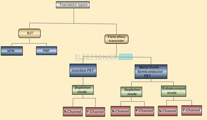
### Types of Junction Transistor
There are two basic types of transistors, which are **NPN** and **PNP**. These transistors have opposite polarity between collector and emitter.
**NPN transistors**
- Allow electricity to pass from the collector pin to the emitter pin.
- They are represented in a schematic with a line for a base, a diagonal line connecting to the base, and a diagonal arrow pointing away from the base.

**PNP transistors**
- Allow electricity to pass from the emitter pin to the collector pin.
- They are represented in a schematic with a line for a base, a diagonal line connecting to the base, and a diagonal arrow pointing towards the base.

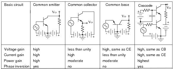
### Transistor Configurations
### Cut off, Active & Saturation Region of Transistor

**1. Cut-off region**
- When load line intersect IB = 0, it is known as cut off region of the transistor.
- As the base current is zero, only small collector leakage current flows. The base emitter junction does not remain in the forward biased because the base current is zero.
- The collector to emitter voltage is equal to VCC.
**2. Saturation region**
- When the load line intersect IB = IB ( saturation ) , it is known as saturation region of the transistor.
- As the base current is maximum, the collector current also becomes maximum.
- The collector to emitter junction does not remain in the reverse biased condition therefore the transistor action is also lost.
- If the base current increases beyond saturation level, the collector current does not increase because of collector to base junction is not remain reverse biased.
IC = VCC / RC
VCE = VCE ( knee )
**3. Active region**
- It is a region between active and cut off of the transistor output characteristic.
- The base to emitter junction remains in forward biased condition whereas the collector to emitter junction remains in the reverse biased condition.
### Current During Different Transistor Region
**1. Active region**
- Collector current IC = βIB
- The transistor works as an amplifier in the active region
**2. Cut off region**
- As there is no base current, the collector current also becomes zero.
**3. Saturation region**
- The transistor behaves as a closed switch between collector and emitter. The collector – emitter path is short circuited.
- Every transistor consists of two diodes emitter – base diode and collector to emitter diode in the common emitter configurations.
| Region | Base-emitter diode | Emitter-collector diode |
| :----: | :----------------: | :---------------------: |
| Cut off | OFF | OFF |
| Saturation | ON | ON |
| Active | ON | OFF |
### Transistor as a Switch
#### A. Cut Off State (Open Switch)


When transistor operates in the cut off region shows the following characteristics
- The input is grounded i.e. at zero potential.
- The VBE is less that cut – in voltage 0.7 V.
- Both emitter – base junction and collector – base junction are reverse biased.
- The transistor is fully – off acting as open switch.
- The collector current IC = 0 A and output voltage Vout = VCC.
#### B. Saturation State (Closed Switch)


The transistor operating in the saturation region exhibits following characteristics −
- The input is connected to VCC.
- Base – Emitter voltage is greater than cut – in voltage (0.7 V).
- Both the base – emitter junction and base – collector junction are forward biased.
- The transistor is fully – ON and operates as closed switch.
- The collector current is maximum and IC= (VCC/ Rl) and Vout = 0 V.
### Identification factor
- Transistors have their part number printed on them and you can look up their datasheets online to learn about their pin layouts and their specific properties.
- Be sure to take note of the transistor's voltage and current rating as well.
## MOSFET
- The **metal–oxide–semiconductor field-effect transistor** (**MOSFET**, **MOS-FET**, or **MOS FET**) is a type of field-effect transistor (FET).
- It has an insulated gate, the voltage of which determines the conductivity of the device.
- This ability to change conductivity with the amount of applied voltage can be used for amplifying or switching electronic signals.
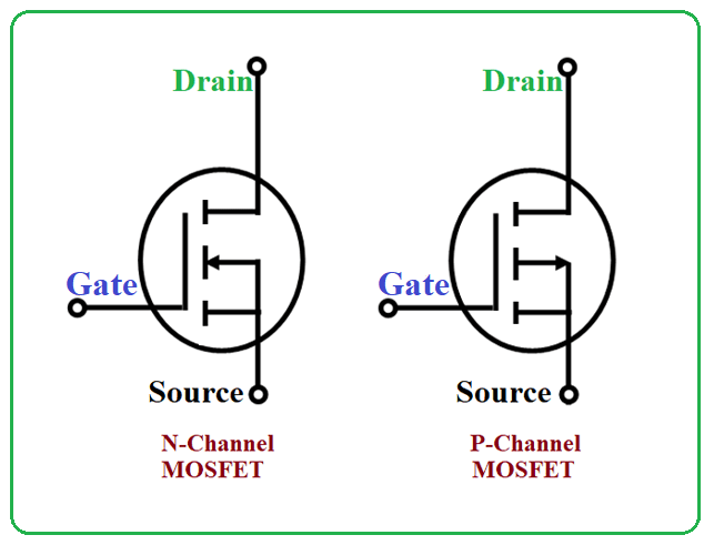
MOSFETs also have three terminals, namely Drain (D), Source (S) and Gate (G) and also one more (optional) terminal called substrate or Body (B).
MOSFETs are also available in both types,
N-channel (NMOS) and P-channel (PMOS).
MOSFETs are basically classified in to two forms. They are:
**1. Depletion Type**
**2. Enhancement Type**
#### Depletion Type
- The depletion type MOSFET transistor is equivalent to a “normally closed” switch.
- The depletion type of transistors requires gate – source voltage (VGS) to switch OFF the device.

- In this type of MOSFETs a thin layer of silicon is deposited below the gate terminal.
- The depletion mode MOSFET transistors are generally ON at zero gate-source voltage (VGS).
- The conductivity of the channel in depletion MOSFETs is less compared to the enhancement type of MOSFETs.
#### Enhancement Type
- The Enhancement mode MOSFET is equivalent to “Normally Open” switch and these types of transistors require a gate-source voltage to switch ON the device.
- The symbols of both N-channel and P-channel enhancement mode MOSFETs are shown below.
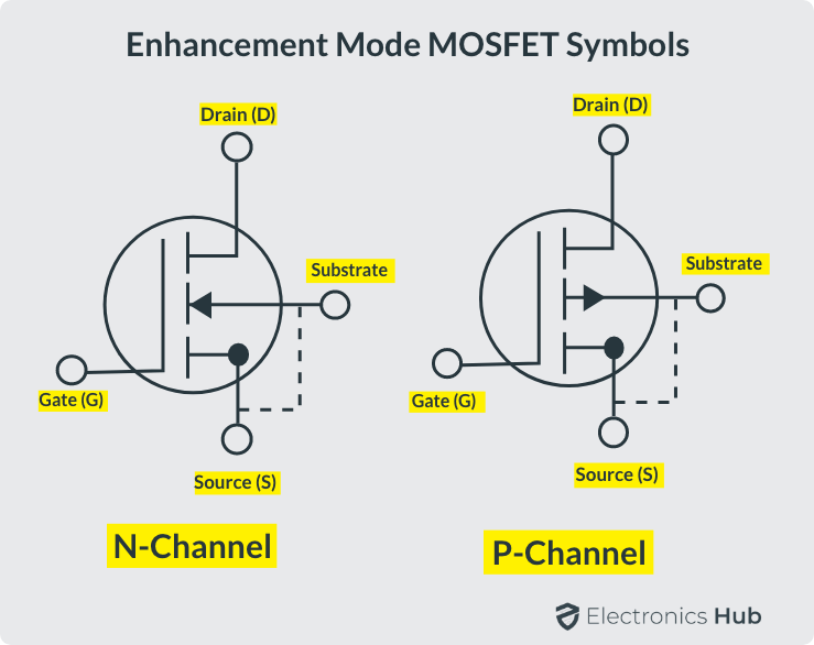
- Generally, this oxide layer is called as ‘Inversion layer’.
- The channel is formed between the drain and source in the opposite type to the substrate, such as N-channel is made with a P-type substrate and P-channel is made with an N-type substrate.
- The conductivity of the channel due to electrons or holes depends on N-type or P-type channel respectively.
### Application of MOSFET
- Mosfet is used for some switching applications an in electronics device.
- It is used in some amplifying circuits.
- MOSFET can be used as a high-frequency amplifier.
- It can be used in voltage regulator circuits.
- It is used as an inverter in some of the electronics circuits.
- It can be used as a passive element e.g. resistor, inductor used in a circuit.
- It is used in SMPS ( switch mode power supply ).
- It is used in some DC brushless motor drives.
- It is used in DC relay in electronics.
- It can be used in digital circuits
### MOSFET application as a Switch
- As above we saw there are two types of MOSFET. Here we know the application of MOSFET using Enhancement type MOSFET.
- In this circuit, we are using enhancement mode, an N-channel MOSFET is being used to switch the LED or LAMP for ON and OFF.

- The voltage is applied at the gate of the MOSFET at that condition the lamp is ON.
- When the zero voltage level is applied at the gate then the device and lamp is turned off (VGS=0.
- So by this way, we can use MOSFET for switching operation. And MOSFET has a very high switching device.
## BJT vs MOSFET
| Parameter | BJT | MOSFET |
| --- | ---| --- |
|Full form | BJT stands for Bipolar Junction Transistor. | MOSFET stands for Metal Oxide Semiconductor Field Effect Transistor.|
| Definition | BJT is a three-terminal semiconductor device used for switching and amplification of signals.| MOSFET is a four-terminal semiconductor device which is used for switching applications.|
| Types | Based on the construction, BJTs are classified into two types: NPN and PNP. | Based on the construction and operation, the MOSFETs are classified into four types: P-channel enhancement MOSFET, N-channel enhancement MOSFET, P-channel depletion MOSFET and N-channel depletion MOSFET.
| Terminals | BJT has three terminals viz. emitter, base and collector. | MOSFET has four terminals, i.e., source, drain, gate and body (or substrate).
| Charge carriers | In BJT, both electrons and holes act as charge carriers. | In MOSFET, either electrons or holes act as charge carriers depending on the type of channel between source and drain.
| Polarity | BJT is a bipolar device. | MOSFET is a unipolar device.
| Controlling quantity | BJT is a current controlled device. | MOSFET is a voltage controlled device.
| Input impedance|BJT has low input impedance. | MOSFET has relatively high input impedance.
|Temperature coefficient | BJT has negative temperature coefficient. | MOSFET has positive temperature coefficient. |
| Switching frequency | The switching frequency BJT is low.|For MOSFET, the switching frequency is relatively high.
| Power consumption | BJT consumes more power than MOSFET. | The power consumed by a MOSFET is less than BJT
| Applications | BJT is preferred for the low current applications. It is widely used as amplifiers, oscillators and electronic switches.| MOSFET is suitable for high power applications. It is used in power supplies, etc.
### Switch Debouncer:

#### Switch Debounce waveform:

#### Hardware solution:

### Pull-Up and Pull-Down Resistor:
- Pull-up and Pull-Down Resistors used in digital systems.
- In a digital system, there are three states:

- Two obvious states are Logic High and Logic Low. But suppose if we left any pin unconnected/floating then it is said to be tristate or unknown.
- Example of this in popular 7432 OR gate IC's datasheet:

- Range [2V - 5V]: considered as Logic HIGH.
- Range [0 - 0.8V]: considered as Logic LOW.
- Range [0.8 - 2V]: considered as indeterminate state.

- If we try to measure simple digital input of a micro-controller without any precaution for this unknown state then input signal will look like this:

- But if we connect a pull-up resistor at the input of micro-controller then input signal will look something like this:

### FlipFlops and Latches:
- FlipFlops and Latches are the building blocks of most sequential circuits. FlipFlop is a device that samples it's input and changes only when a clock signal changes. On the other hand latches are sequential devices that watch it's inputs continuously and can change its outputs at any time.
#### Latches
- SR Latch
- There are 2 types of SR latches depending on the gates used :-
1) SR Latch ( with NOR gates )

2) SR Latch ( with NAND gates )

### FlipFlops
#### SR FlipFlop
- One extra signal is used here and it is a control signal like the clock signal.

#### D FlipFlop
- **What if we go into the invalid state by mistake???**
The data will be lost and we do not want that.
We can see that if we make S and R complements of each other then the invalid state is removed. That is a problem as we can't access the S=0 and R=0 state i.e the memory state.
**What can you do?**
Actually this is not a problem as you have clock signal. If you make the clock signal 0 then you automaticaly go into memory state.

# Measurement Instruments:
## Digital Multimeter
### Manual:

- In manual DMM you have to set the range of readings manually.
**Method:**
#### DC voltage:
- Insert **BLACK** probe in common/negative/ground terminal of DMM and **RED** terminal in positive terminal.
- Set the knob on appropriate **DC voltage range**
- Measure the voltage without touching your hands to probe.
#### AC voltage /DC current:
- Follow the same steps mentioned above
#### Resistance:
- Estimate the value of resistance using color code
- Insert **BLACK** probe in common/negative/ground terminal of DMM and **RED** terminal in positive terminal.
- Set the knob on appropriate **Resistance range**
- Measure the voltage without touching your hands to probe.
#### 10A/20A mode:
- Some DMMs can have a dedicated mode to measure higher DC current. In this mode, the fuse of DMM is bypassed. Thus the DMM can damage if high current is flowing through it for a longer duration (Read the specifications mentioned on DMM).
- To measure in this mode, Insert **BLACK** probe in common/negative/ground terminal of DMM and **RED** terminal in dedicated terminal.
#### Continuity/ Diode test/ LED:
- Insert **BLACK** probe in common/negative/ground terminal of DMM and **RED** terminal in positive terminal.
- Set the knob on **Continuity mode**
**Continuity**:
Listen for the buzzer sound.
**Diode test**:
The display will show the forward bias resistance.
**LED**:
LED will turn on and display will show forward bias resistance.
#### Transistor test:
- Set the knob on transistor test/ hFE mode.
- Insert the transistor in appropriate transistor tester terminals.
- Display will show the current gain (beta value/hFE parameter) of the transistor.
#### Precautions:
- It is always advised to set the range one step higher than estimated reading. For example if the estimated reading is 18V then first measure the voltage using the 200V option and then if the reading is below 20V, you can switch to the 20V range.
- Extra care should be taken while measuring higher voltage or current.
- While taking readings, don’t touch your hands to DMM probes. It may cause hazards or errors in readings.
### Automatic:
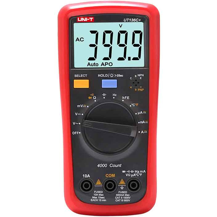
- In these multimeters, the user doesn’t need to set the range.
- To measure, insert DMM probes in appropriate terminals, set the knob on the quantity which you want to measure.
Measure the quantity, wait till the readings stabilize.
## Oscilloscope:
- Horizontal controls used to adjust time axis
- Vertical controls used to adjust amplitude of signal
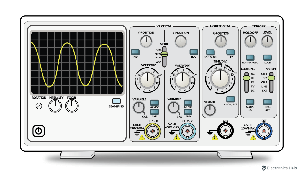
Oscilloscope is a powerful tool used to visualize signals, waveforms as a function of time. It can be used to analyze frequency, amplitude, rise time, time interval and distortions of signals.
[Do check out this link on how to use an Oscilloscope!](https://www.youtube.com/embed/u4zyptPLlJI)
#### Functions:
- Cursors
- Protocol decoding
- Mathematical functions like addition/subtraction
- Measure (automatically measure time period, frequency, amplitude)
- Auto (auto adjust time scale and voltage scale)
***
# PCB Designing
## Importance of PCBs
- Eminent PCB manufacturers such as PCB Power make PCBs from thin insulating boards with a coating of metal on one or both sides. PCBs hold almost all the electronic components necessary for a device to function. Fabricators etch the metal with acid to create electrical pathways among various components that assemblers mount on the board. Using a PCB brings many advantages to the electronic industry:
1. Compact Design
2. Ease of Testing and Repair
3. Lower Assembly Errors
4. Avoiding Short Circuits
5. Low Noise and Interference
6. Improved Repeatability and Reliability
## But why to design PCBs?
- Early radio receivers built using valves had a metal chassis for mounting the valves, dials and switches.
- Since the total number of components were very few, and all were with leads, it was easy to solder them while they hung from terminal boards and interconnect them with wires.
However, this procedure became a nightmare when circuit complexity grew and the number of components increased. Using Printed Circuit Boards (PCBs) is a solution to this problem.
## Types of PCBs
- Printed circuit boards (PCBs) are the heart of all electronic products, but not all are created equal.
Below is a list of the common types of printed circuit boards.
### 1. Single Layer PCB
- Single layer printed circuit boards are among some of the simplest to design and manufacture.
These boards have a single layer of conductive material (such as copper) on only one side of a non-conductive substrate.
### 2. Double Layer PCB
- Double layer PCBs have one conductive layer on top of a non-conductive substrate and another conductive layer on the reverse side (top and bottom layers).
- The two conductive sides can be connected using plated holes in the substrate that connect to pads on both sides of the circuit board; these are called vias.
### 3. Multi-Layer PCB
- This term refers to a circuit board that has three or more conductive layers.
- The conductive layers are at the top and bottom, as well as at least one conductive layer sandwiched between non-conductive substrate
the most commonly used have lower layer counts such as 4, 6, or 8 layer boards.
### 4. High Density Interconnect (HDI) PCB
- HDI PCBs take advantage of precision based manufacturing technology to pack as much functionality into a small space.
- This is done by using many conductive layers, laser drilled microvias, fine lines and tolerances, and advanced laminate materials.
HDI PCBs can accommodate the complex routing of high pin count chips and other high-tech miniaturized components.
## Types of components PCB is designed for
### 1. Dual In-line Package (DIP):

- A dual in-line kit is a digital part kit with a pyramid shape and the electrical connecting pins in two parallel rows. The product is installed or placed in a socket on a circuit board.
### 2. Surface Mounted Devices (SMD):
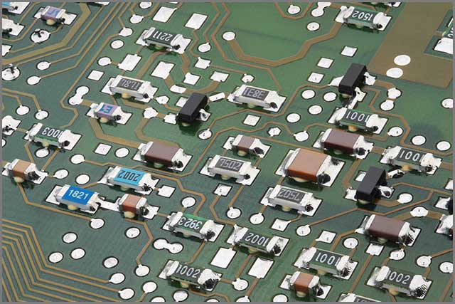
- Texture mounting technology (SMT) is a means by which electronic circuits are installed or positioned adsorbed on the surface of circuit boards such as PCBs.
This is called the surface mounting system an electrical device SMD Service.
## Basic Softwares Used

**KiCad EDA**
- KiCad is a free and open-source electronics design automation (EDA) suite.
- It features schematic capture, integrated circuit simulation, printed circuit board (PCB) layout, 3D rendering, and plotting/data export to numerous formats.
- KiCad also includes a high-quality component library featuring thousands of symbols, footprints, and 3D models.
#### Schematic Capture
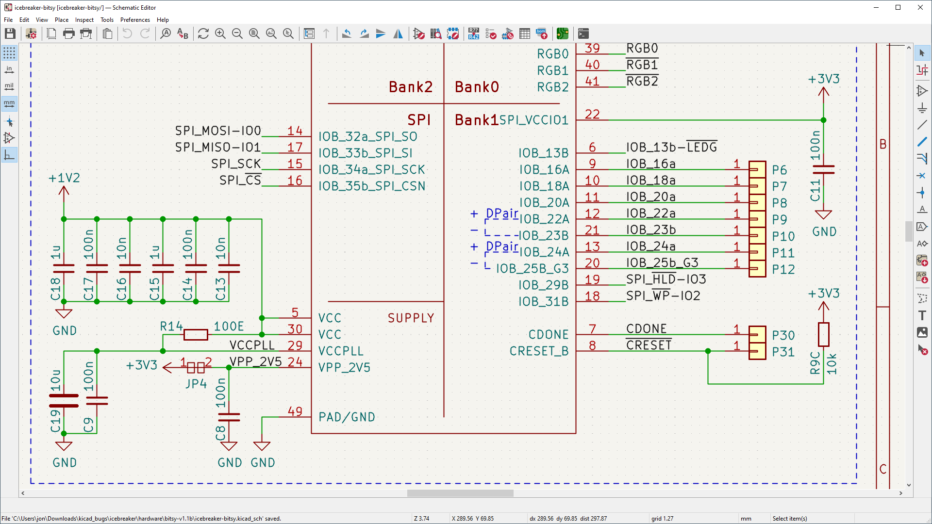
**KiCad's Schematic Editor**
- Supports everything from the most basic schematic to a complex hierarchical design with hundreds of sheets.
- Create your own custom symbols or use some of the thousands found in the official KiCad library. Verify your design with integrated SPICE simulator and electrical rules checker.
#### PCB Layout
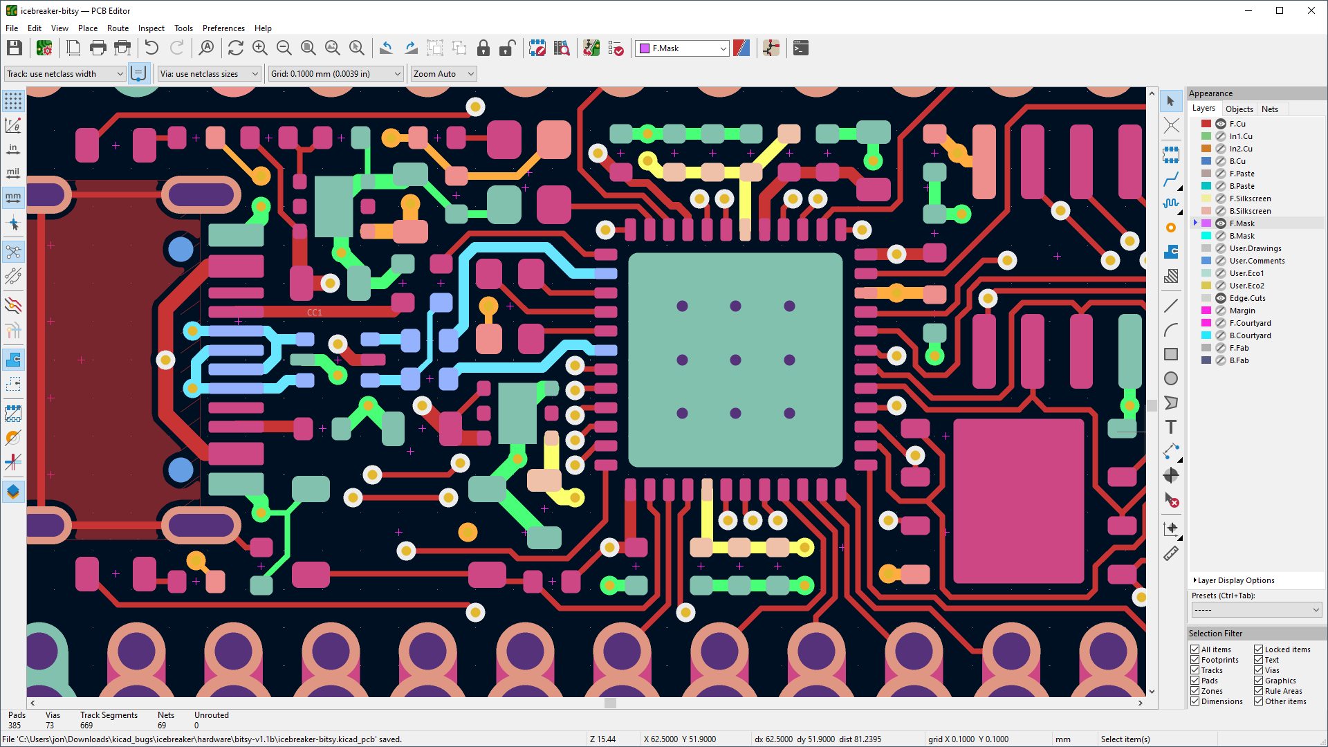
**KiCad's PCB Editor**
- Is approachable enough to make your first PCB design easy, and powerful enough for complex modern designs. A powerful interactive router and improved visualization and selection tools make layout tasks easier than ever.
#### 3D Viewer
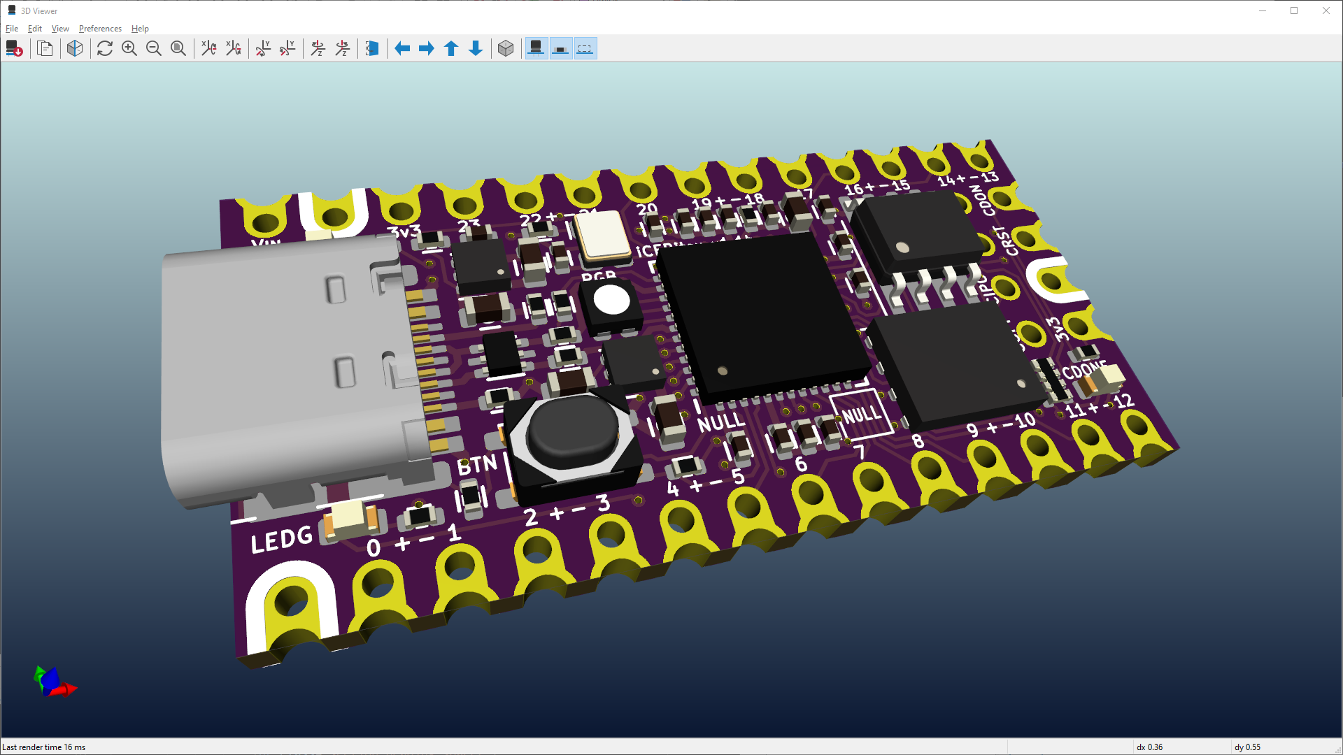
**KiCad's 3D Viewer**
- Allows easy inspection of your PCB to check mechanical fit and to preview your finished product. A built-in raytracer with customizable lighting can create realistic images to show off your work.
## Steps to design a PCB
The process flow for designing a PCB shows four major steps:
### 1. Requirements Gathering
- This is the input stage and the designer collects information about the intended functioning of the circuit.
### 2. Schematic Design
- In the next stage, the designer draws the circuit and creates an orderly schematic that represents the logical functioning of the circuit.
- The software module handling the schematic drawing assigns individual part numbers to each component and interprets the interconnections to and from their pins as part of a net. The designer must assign a valid footprint to each part in the schematic.
After completion of the schematic design, the software module offers two outputs:
#### 1. A Bill of Materials (BOM) and
- The BOM is a complete list of all the components the designer has used to build the schematic. The organization uses this BOM to source the components.
#### 2. Net List.
- The net list is an important document that the designer uses to layout the components for routing.
- The net list ensures that the designer faithfully transfers all interconnections in the schematic to the layout before starting on the routing.
### 3. Component Placement

- The designer must carefully select the correct footprint, as a component may be available in several forms such as through-hole and surface mount types.
- The designer must place each component such that it can function properly either within the specified boundary of the PCB or within a minimum area.
### 4. Routing and Output Generation
- In the final stage, the designer invokes the routing module of the CAD package.
This module usually has two parts— **the auto-router** and the **manual router**.
- The auto-router uses algorithms to create traces while routing them through the components.
- If the designer wants, they can use the manual router to manually create the traces, rather than allowing the computer to create them automatically.
- For a complex design, the designer may have to shuttle between placement and routing until they achieve a satisfactory compromise.
- On completion, they generate the necessary standard outputs, which they forward for fabricating Primarily, fabricators require Gerber data, drill information, a netlist, and specific fabrication instructions to start manufacturing a board.
---
**Assignment 1**
- Find out values of different SMD components on the SRA Board.
- Check continuity.
- Observe output waveform of the PWM signal on Oscilloscope.